
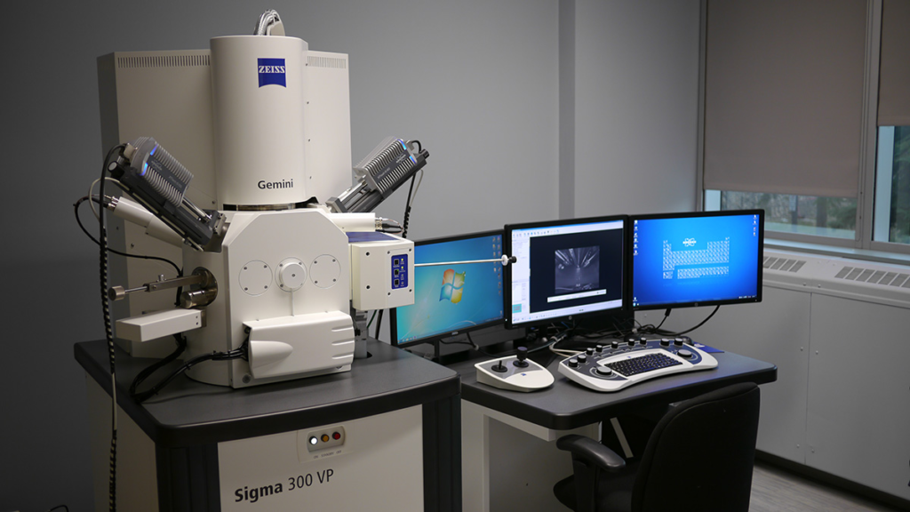
Scanning Electron Microscope
A Scanning Electron Microscope (SEM) is an advanced imaging tool that uses focused beams of electrons to scan the surface of a sample, producing high-resolution, detailed images at the micro or nanoscale. Unlike optical microscopes that use light, SEMs provide much greater magnification and depth of field, allowing for precise visualization of surface topography and composition. When the electron beam interacts with the sample, it generates various signals, including secondary electrons, backscattered electrons, and X-rays, which are detected to produce images and elemental composition maps. This makes SEMs highly valuable in fields like materials science, geology, biology, and nanotechnology, where understanding fine-scale surface features is crucial.
====================================================================
Download the presentation here:
++++++++++++++++++++++++++++++++++++++++++++++++++++++++++++++++++++
Basic Principle:
An SEM generates images by scanning the surface of a specimen with a focused beam of electrons. Unlike a conventional light microscope, which uses photons, an SEM uses electrons. These electrons interact with the sample’s surface, and the resulting signals provide detailed information about its morphology, composition, and other properties.
Electron-Sample Interaction:
- As the high-energy electrons from the SEM beam hit the sample, they interact with the atoms within the material.
- This interaction produces several signals, including secondary electrons, backscattered electrons, characteristic X-rays, and other emissions.
- Each signal carries specific information:
- Secondary electrons (SEs) are commonly used to generate high-resolution images, revealing surface topography (i.e., the fine details of the sample’s surface).
- Backscattered electrons (BSEs) provide contrast based on the atomic number, so heavier elements appear brighter in the image compared to lighter elements.
- X-rays emitted from the sample can be used to perform elemental analysis, which is the basis of energy-dispersive X-ray spectroscopy (EDS or EDX).
Image Formation:
- The SEM’s electron beam is scanned across the sample in a raster pattern, where it moves line by line over the sample’s surface.
- As it scans, the Everhart-Thornley detector collects the emitted secondary electrons, converting their signal into a visual image.
- The brightness or intensity of the image corresponds to the amount of secondary electrons detected, which depends largely on the surface topography and the composition of the sample.
Resolution:
- SEMs can achieve very high resolutions, with modern instruments able to image features as small as 1 nanometer. The resolution depends on the size of the electron beam, which can be made extremely small due to the shorter wavelength of electrons compared to light.
- The resolution is also influenced by factors like the electron accelerating voltage, the type of sample, and how it interacts with the electron beam.
Specimen Environment:
- In a conventional SEM, the sample must be placed in a high vacuum to prevent the scattering of electrons by air molecules.
- For more sensitive or non-conductive samples, variable pressure or environmental SEMs (ESEM) allow samples to be imaged in low vacuum conditions, or even in the presence of a gaseous environment (which can be used for wet samples or hydrated biological specimens).
- Cryogenic SEMs can image samples at extremely low temperatures, useful for biological materials, which are susceptible to damage or changes under the electron beam. Conversely, specialized SEMs can work at elevated temperatures to study materials under conditions such as heating or oxidation.
Surface Topography and Composition:
- Topography: Secondary electrons are very sensitive to the surface structure of the sample, providing detailed three-dimensional images of the surface. For example, samples with rough or inclined surfaces will produce more secondary electrons than flat surfaces, which leads to brightness variation in the image that reveals the surface’s contours.
- Composition: With the help of backscattered electron detectors and X-ray analysis systems (EDS/EDX), SEM can provide insights into the elemental composition of the sample. Heavier elements tend to reflect more electrons (resulting in brighter regions in the image), which allows differentiation between regions with different elemental compositions.
- _________________________________________________________
Different types of microscopy techniques are used to analyze a geological sample. In electron microscopy, we have three main types of detection.
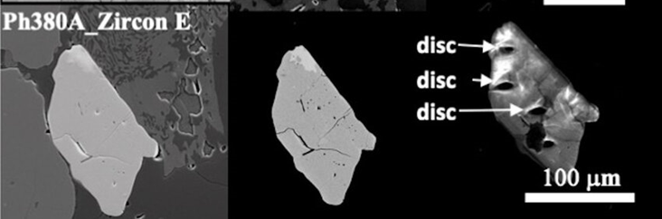
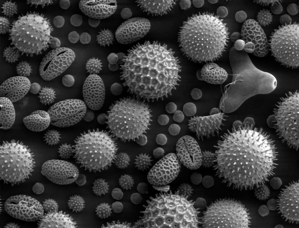
- Secondary electron (a): The first image is a secondary electron (SE) micrograph from a scanning electron microscope (SEM). This imaging mode primarily captures surface topography by detecting low-energy secondary electrons emitted from the surface atoms of the sample. Secondary electron images are highly sensitive to surface detail, highlighting fine textures and features such as grain boundaries, cracks, and surface roughness. In this case, the SE image reveals detailed structural features of the sample’s surface, showcasing the morphology and the arrangement of particles, giving a three-dimensional appearance that allows for analysis of the microstructure at a high resolution.
- Backscattered electron (b): The second image is from a backscattered electron (BSE) detector in a scanning electron microscope (SEM). It contrasts areas of the sample based on atomic number, with lighter regions indicating elements with higher atomic numbers and denser compositions. This image shows clear structural differences between the core and rim of the grain.
- Cathodoluminescence (c): The third image is from cathodoluminescence (CL) imaging, which highlights different luminescent properties of minerals when they are bombarded by an electron beam. It reveals growth zoning within the mineral, indicating variations in chemical composition during formation. This technique is especially useful for identifying trace elements and growth patterns not visible under normal light.
All three images provide complementary data on the composition, structure, and growth history of the mineral grain. With an SEM we can collect Backscattered and Cathodoluminescence images at the same time.
Advantages of SEM:
- High resolution: SEMs can resolve very fine surface features, providing a much higher level of detail than optical microscopes.
- Depth of field: SEM images have a large depth of field, which means that even rough or uneven surfaces can be imaged sharply across the field of view.
- Versatile imaging conditions: With the ability to operate in high vacuum, low vacuum, or environmental modes, SEMs can image a wide variety of materials, from metals and semiconductors to biological tissues and wet samples.
Applications:
- SEM is used in numerous fields, including material science, biology, forensics, nanotechnology, and geology.
- In material science, it helps analyze fracture surfaces, corrosion, and microstructural features of metals and polymers.
- In biology, SEM can visualize cell structures and tissue morphology at very high resolutions.
- In geochronology or mineralogy, SEM is useful for analyzing the surface characteristics and composition of minerals.
In summary, SEM is a powerful tool that combines detailed surface imaging with elemental composition analysis, making it indispensable in scientific research and industrial applications for understanding the microscopic and nanoscale properties of materials.
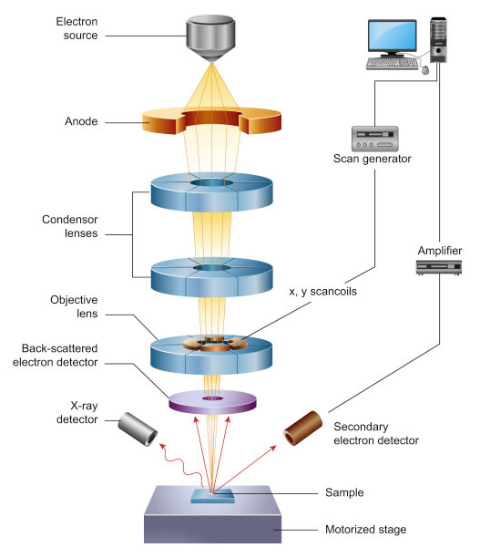
How SEM Works:
- Electron Beam Generation:
- The SEM uses a finely focused beam of high-energy electrons (typically 1-30 kV) generated by an electron gun, usually a tungsten filament, a lanthanum hexaboride (LaB6) crystal, or a field emission gun (FEG).
- The electron beam is accelerated and focused using electromagnetic lenses to form a narrow, high-intensity beam.
- Scanning the Sample:
- The focused electron beam is scanned across the surface of the sample in a raster pattern. This scanning action allows the SEM to build up a detailed image of the surface by collecting information from each point where the beam interacts with the sample.
- Electron-Sample Interactions:
- When the high-energy electron beam strikes the sample, a variety of interactions occur, producing different signals that can be detected to form images and gather compositional information:
- Secondary Electrons (SE): These are low-energy electrons emitted from the sample’s surface due to inelastic collisions between the incoming electrons and the sample’s atoms. Secondary electrons provide high-resolution images of the sample’s surface topography.
- Backscattered Electrons (BSE): These are high-energy electrons from the primary beam that are elastically scattered back from the sample. BSE signals are often used to generate compositional contrast images because heavier elements backscatter more electrons, appearing brighter in BSE images.
- X-rays: When the electron beam excites the atoms in the sample, they emit characteristic X-rays. These X-rays can be detected and analyzed through Energy-Dispersive X-ray Spectroscopy (EDS/EDX) to determine the elemental composition of the sample.
- When the high-energy electron beam strikes the sample, a variety of interactions occur, producing different signals that can be detected to form images and gather compositional information:
- Detection and Imaging:
- Various detectors are used to capture different types of signals produced by the electron-sample interactions:
- Secondary Electron Detector: This detector collects secondary electrons and is used to produce detailed images of the sample’s surface topography.
- Backscattered Electron Detector: This detector collects backscattered electrons and provides images that show compositional contrast.
- X-ray Detector: An energy-dispersive detector is used to analyze the characteristic X-rays for elemental composition mapping.
- Various detectors are used to capture different types of signals produced by the electron-sample interactions:
- Image Formation:
- The intensity of the detected signals (secondary electrons, backscattered electrons, or X-rays) is mapped to a grayscale image, where the contrast represents differences in surface texture, material composition, or other properties of the sample.
Key Features of SEM:
- High Resolution and Magnification:
- SEM can achieve very high magnifications (from about 10x to over 100,000x) with a resolution down to a few nanometers, allowing for detailed analysis of very small surface features.
- Three-Dimensional Surface Imaging:
- By collecting secondary electrons, SEM provides detailed three-dimensional images of a sample’s surface, making it possible to observe features such as cracks, fractures, and surface textures.
- Elemental Analysis with EDS/EDX:
- SEM can be equipped with Energy-Dispersive X-ray Spectroscopy (EDS/EDX) detectors to analyze the X-rays emitted by the sample during electron bombardment. This allows users to determine the elemental composition of the sample and create elemental maps showing the distribution of elements across the surface.
- Backscattered Electron Imaging:
- The BSE detector allows for compositional contrast imaging. Heavier elements appear brighter in BSE images, while lighter elements appear darker. This can be useful for distinguishing between different phases or materials within a sample.
Sample Preparation for SEM:
- Conductive Coating:
- SEM requires that samples be electrically conductive, or at least coated with a thin layer of conductive material (such as gold, platinum, or carbon) to prevent the buildup of electric charge on the surface during imaging. Non-conductive samples (like biological specimens or ceramics) are typically sputter-coated with a conductive layer before examination.
- Vacuum Requirement:
- The SEM chamber must operate under a high vacuum to prevent the electron beam from interacting with air molecules. This means that samples must be dry and stable under vacuum conditions. Biological samples, for instance, need to be dehydrated or cryogenically frozen for imaging.
Limitations of SEM:
- Vacuum Requirement:
- SEM needs to operate under a vacuum, limiting the types of samples that can be analyzed. Biological and hydrated samples often need special preparation techniques (such as dehydration or freezing) to be examined.
- Sample Conductivity:
- Non-conductive samples need to be coated with a conductive material before imaging, which can introduce artifacts or mask very fine surface details.
- Limited Penetration Depth:
- SEM primarily provides surface information, as the electron beam interacts only with the top few micrometers of the sample. Subsurface features cannot be directly imaged with SEM.
- Lower Resolution than TEM:
- While SEM provides high resolution, it generally cannot match the atomic-level resolution of Transmission Electron Microscopy (TEM), which is capable of imaging individual atoms.
Applications of SEM:
- Materials Science:
- SEM is widely used to analyze metals, alloys, ceramics, and polymers for surface defects, grain structure, fractures, and corrosion.
- Biology and Medicine:
- Biological samples, such as tissues and cells, can be imaged using SEM to study their surface morphology, though careful sample preparation is required.
- Geology:
- SEM is employed to study the surface texture and composition of minerals, rocks, and fossils, often in combination with EDS/EDX to perform elemental analysis.
- Semiconductor and Microelectronics Industry:
- SEM is crucial for inspecting and characterizing microelectronic devices and components, where precise surface imaging and defect analysis are essential.
- Forensics:
- SEM is used in forensic science to examine small particles, fibers, gunshot residues, and other trace evidence that requires high-resolution surface imaging and elemental analysis.
Summary:
The Scanning Electron Microscope (SEM) is an essential tool in modern science and engineering for imaging the surface of materials with nanometer-level resolution. It works by scanning a focused beam of electrons over a sample and collecting signals such as secondary electrons, backscattered electrons, and X-rays. SEM produces detailed, three-dimensional images of a sample’s surface topography and can be combined with elemental analysis through EDS/EDX. While it has limitations related to sample preparation and vacuum requirements, SEM is invaluable across numerous disciplines for high-resolution surface analysis and material characterization.
SPECIAL FEATURES
1. EDX – MAPPING
Energy Dispersive X-ray Spectroscopy (EDX) Mapping, also known as EDS Mapping, is a technique used to visualize the spatial distribution of elements in a material or sample. This method is widely employed in combination with Scanning Electron Microscopy (SEM) or Transmission Electron Microscopy (TEM) to provide detailed elemental composition information.

EDX mapping is especially useful in geological studies, materials science, and metallurgy for understanding the distribution of different elements within samples.
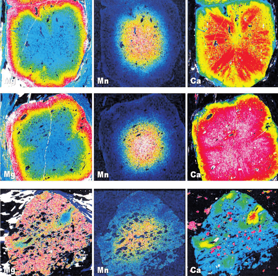
In the above image, we have the distribution of Mg, Mn, and Ca detected by EDX. The EDX mapping clearly visualizes the spatial distribution of these elements within the mineral grains:
- Mg maps reveal magnesium-rich areas, indicating zones where Mg was more prevalent during crystallization.
- Mn maps highlight manganese concentrations, often located in the core or rim of the grain, providing insights into the growth history.
- Ca maps show calcium-rich regions, frequently forming at the edges of the grains, likely indicating secondary growth or recrystallization
Key Features of EDX Mapping:
- How It Works:
- An electron beam from the SEM or TEM bombards the sample.
- The interaction between the electron beam and the atoms in the sample causes X-rays to be emitted. Each element emits characteristic X-rays at specific energy levels.
- The EDX detector identifies these X-rays and maps their intensity, correlating the X-rays with the elements in the sample.
- Mapping Process:
- The electron beam is rastered across the sample in a grid pattern.
- As the beam interacts with different regions, the detector measures the X-ray emissions and determines which elements are present at each location.
- These measurements are then used to produce a colour-coded map where each colour corresponds to a different element.
- The maps show the spatial distribution of elements, allowing researchers to visualize which parts of the sample contain specific elements, whether elements are uniformly distributed, or if they are concentrated in specific areas (such as cores, rims, or fractures).
- Applications:
- Geology: EDX mapping can identify zoning in minerals, where different elements (like magnesium, calcium, and iron) are concentrated in various layers, revealing information about the formation conditions of rocks and minerals.
- Materials Science: It is used to study alloys, ceramics, and composites to see how different elements are distributed in these materials, which can be critical for understanding properties like hardness, durability, and resistance to corrosion.
- Metallurgy: EDX maps help in studying inclusions or contaminants within metals, the distribution of alloying elements, and the microstructure of metallic phases.
- Data Interpretation:
- Uniform Distribution: If an element is uniformly distributed, it indicates that the sample material is homogeneous for that particular element.
- Zoning: EDX mapping can show chemical zoning, where elements vary from the core to the rim of grains, revealing information about the growth history of minerals.
- Segregation or Clustering: Areas of higher concentration (bright spots on the map) may indicate phases rich in that element, inclusions, or areas where that element has segregated during cooling or crystallization.
- Limitations:
- EDX is a surface-sensitive technique, and its spatial resolution is limited by the interaction volume between the electron beam and the sample. The resolution can range from nanometers to micrometres, depending on the instrument and settings.
- Elements with very low atomic numbers (e.g., hydrogen, lithium) cannot be detected with EDX, as their X-rays are too weak to be distinguished.
- EDX is generally qualitative or semi-quantitative. While it can identify the presence and relative concentration of elements, precise quantification requires careful calibration and additional methods.
Example of EDX Mapping:
In the image below we have a detailed EDX (Energy Dispersive X-ray Spectroscopy) analysis of sand grains. It provides both elemental mapping and quantitative data about the sample’s composition, utilizing an SEM (Scanning Electron Microscope) for structural visualization and elemental identification. Here’s a breakdown of the different parts:
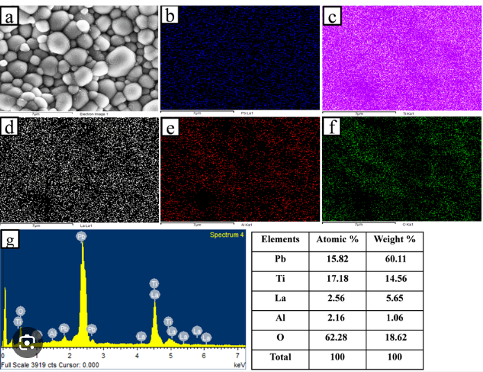
a) SEM Image:
- This is a grayscale electron micrograph (SEM) showing the structure of the sample at the micrometer scale. The sample appears to be composed of spherical particles, possibly representing a powder or granulated material. The high contrast helps reveal the sample’s surface topography.
b–f) Elemental Maps:
- These color-coded maps show the distribution of different elements in the sample, generated by the EDX detector. Each map corresponds to a specific element:
- b (Pb Map, Blue): Shows the distribution of lead (Pb) in the sample. The blue regions indicate where Pb is concentrated, which appears to be relatively uniform.
- c (Ti Map, Magenta): Displays the titanium (Ti) concentration. Ti is evenly distributed throughout the sample, which is indicated by the magenta color.
- d (La Map, White): This map represents the distribution of lanthanum (La). The white spots indicate areas with higher La content, which seems uniformly scattered.
- e (Al Map, Red): Shows aluminum (Al) content. Red areas correspond to regions rich in Al, suggesting the element is also widely spread across the sample.
- f (O Map, Green): The green map reveals the presence of oxygen (O). The high concentration of green across the sample suggests that the material contains significant oxides or oxygen-rich compounds.
g) EDX Spectrum:
- This spectrum shows the X-ray energy peaks corresponding to the elements detected in the sample. Each peak corresponds to a characteristic X-ray emission from an element present in the sample.
- The prominent peaks for Pb (Lead), Ti (Titanium), La (Lanthanum), Al (Aluminum), and O (Oxygen) confirm the presence of these elements.
- The intensity of the peaks indicates the relative abundance of each element, with Pb and Ti showing stronger peaks, indicating higher concentrations.
Table: Elemental Quantification:
- The table lists the elemental composition in terms of both atomic percentage (the proportion of atoms) and weight percentage (the proportion by weight). The values reveal the following composition:
- Pb (Lead): 15.82 atomic % and 60.11 weight % – Pb is the most abundant element by weight, indicating it’s a major component of the material.
- Ti (Titanium): 17.18 atomic % and 14.56 weight % – Ti is significant both in atomic and weight percentages.
- La (Lanthanum): 2.56 atomic % and 5.65 weight % – Present in smaller quantities.
- Al (Aluminum): 2.16 atomic % and 1.06 weight % – Found in lower concentrations.
- O (Oxygen): 62.28 atomic % and 18.62 weight % – Oxygen is abundant, confirming the presence of oxide compounds in the sample.
2. Quantitative Elemental Analises
A Wavelength Dispersive (WD) detector is a key component in Wavelength Dispersive X-ray Spectroscopy (WDS), a technique used to analyze the elemental composition of a material with high precision. Unlike Energy Dispersive X-ray Spectroscopy (EDS), which uses energy differences to identify elements, WDS measures the specific wavelengths of X-rays emitted by the sample, offering better resolution and sensitivity, particularly for elements with closely spaced energy levels.
Key Features of the WD Detector:
- How It Works:
- When a sample is bombarded with an electron beam (typically in an electron microprobe or scanning electron microscope), it emits X-rays as the atoms’ inner-shell electrons are excited and then return to a lower energy state.
- The WD detector analyzes these X-rays by directing them through a diffraction crystal, which separates the X-rays based on their wavelengths according to Bragg’s Law.
- The diffracted X-rays are then measured by the detector, which records their intensity as a function of wavelength.
- Bragg’s Law:
- The detection process is based on Bragg’s Law, which states that X-rays will be diffracted at specific angles depending on their wavelength and the crystal lattice spacing. The equation is: nλ=2dsinθn \lambda = 2d \sin \thetanλ=2dsinθ where:
- n is the order of diffraction (an integer),
- λ is the X-ray wavelength,
- d is the spacing between planes in the diffraction crystal,
- θ is the diffraction angle.
- By measuring the angle at which the X-rays are diffracted, the WD detector can precisely determine the wavelength of the X-rays.
- The detection process is based on Bragg’s Law, which states that X-rays will be diffracted at specific angles depending on their wavelength and the crystal lattice spacing. The equation is: nλ=2dsinθn \lambda = 2d \sin \thetanλ=2dsinθ where:
- High Resolution and Sensitivity:
- WDS systems using WD detectors have higher spectral resolution than EDS detectors, which makes them particularly useful for detecting elements with overlapping X-ray peaks or low concentrations.
- The superior resolution allows WD detectors to distinguish between elements with very similar atomic numbers (e.g., magnesium and sodium, or iron and cobalt), which might not be possible with an EDS system.
- Applications:
- Geology: WD detectors are often used in electron microprobes to perform detailed elemental analysis of minerals. The high precision is essential for identifying trace elements and subtle compositional variations.
- Materials Science: WDS is used to analyze alloys, ceramics, and other advanced materials where precise elemental identification is critical for understanding material properties.
- Environmental Science: WDS can detect low concentrations of toxic elements in environmental samples, providing accurate and reliable data.
- Semiconductor Industry: The technology is used to analyze thin films and materials where the accurate determination of trace elements and impurities is vital.
- Advantages:
- Greater Precision: WD detectors offer greater precision than EDS detectors, especially for low atomic number elements (like boron or lithium) and trace elements present in small quantities.
- Quantitative Analysis: WDS is more suitable for highly quantitative work, making it ideal for research that requires detailed compositional information.
- Lower Detection Limits: WDS can detect elements at lower concentrations (sub-parts per million), which is important for applications like contamination analysis or detecting trace minerals.
- Disadvantages:
- Slower Speed: WDS is generally slower than EDS because it scans each element individually based on wavelength, whereas EDS captures all emitted X-rays simultaneously.
- Complex Instrumentation: WDS systems are more complex and expensive than EDS systems due to the need for diffraction crystals and more sophisticated mechanics.
- Limited Simultaneous Element Detection: Unlike EDS, which can detect all elements present in a sample at once, WDS requires the user to select specific wavelengths (elements) to scan, limiting its ability to detect multiple elements simultaneously.
Typical Setup in Instruments:
- A WD detector is usually integrated into an electron microprobe or an SEM equipped for Wavelength Dispersive X-ray Spectroscopy (WDS).
- These systems often combine EDS and WDS detectors so that researchers can quickly identify the general composition using EDS and then use the WD detector for high-precision analysis of specific elements.
- The diffraction crystals in WD detectors are typically tuned for different ranges of wavelengths, so multiple crystals may be employed to cover a wide range of elements.
Summary:
A WD detector is a highly accurate and precise tool for elemental analysis, particularly useful in applications where exact quantification and the ability to resolve overlapping peaks are crucial. Although it requires more time and complex instrumentation than EDS, WDS provides superior resolution and sensitivity, especially for challenging or trace-level elemental identification.